Laser wafer dicing and traditional wafer dicing differ clearly in principle, process, accuracy, efficiency, and applicability.
Cutting principle and process
Traditional wafer dicing: mechanical cutting with drill bits, saw blades, or blades that directly contact the wafer. Cutting depends on mechanical force. Key parameters include cutting speed, pressure, and cutting depth. Semiconductor materials such as silicon wafers are hard, so mechanical cutting easily wears tools, and parameter adjustment is limited by material hardness and equipment performance.
Laser wafer dicing: a high-energy-density laser beam heats the wafer instantly. Pulsed or continuous laser irradiation creates thermal stress in the material, enabling non-contact cutting. The laser has good monochromaticity and directionality, and can focus to a micron-scale spot. By adjusting beam focus diameter and etching depth, the cutting process is precisely controlled.
Cutting accuracy and quality
Limits of traditional cutting: mechanical cutting has accuracy limits. As chip sizes shrink and wafer diameters grow, it struggles to meet strict production requirements. Cutting easily produces chips and burrs. Chip edge quality drops, and circuit integrity can be affected.
Advantages of laser cutting:
High accuracy: laser spot diameter can be controlled at the micron level, achieving sub-micron cutting accuracy.
No physical contact: avoids mechanical wear and tool replacement, reducing cross-contamination risk.
Stable cutting quality: small heat-affected zone, less thermal damage, smooth chip edges without burrs.
Complex shape cutting: supports curves, irregular shapes, and other non-straight cuts for diverse designs.
Cutting efficiency and output
Efficiency bottleneck of traditional cutting: mechanical cutting speed is limited by equipment rotation speed and material hardness. Worn tools need frequent replacement, increasing downtime. As wafer size grows, single-cut time increases, limiting overall output.
Efficiency gains of laser cutting:
High-speed cutting: laser beam movement speed can reach hundreds of meters per second, far faster than mechanical tools.
Multi-station parallel processing: beam splitting can cut multiple areas at once, raising output per unit time.
Automation integration: easily combines with robots and vision systems for full-process automated production.
Material adaptability and flexibility
Material limits of traditional cutting: mainly for hard materials such as silicon and gallium arsenide. It performs poorly on ultra-thin wafers below 50 μm or composite materials, and easily causes cracking or delamination.
Broad applicability of laser cutting:
Multi-material compatibility: can cut silicon, silicon carbide, glass, ceramics, and other hard and brittle materials, as well as flexible substrates such as polyimide.
Thickness adaptability: by adjusting laser power and pulse frequency, it precisely cuts thicknesses from microns to millimeters.
3D structure processing: supports step cutting, chamfering, and other complex processes for advanced packaging needs.
Equipment and cost considerations
Equipment cost of traditional cutting: mechanical cutting equipment has lower initial investment, but long-term operation requires frequent replacement of drill bits, saw blades, and other consumables. Maintenance cost rises as equipment ages.
Cost of laser cutting:
High initial investment: core components such as lasers and beam delivery systems cost more.
Clear long-term returns: low consumable cost, with only regular laser maintenance. High cutting quality and improved yield can offset the initial investment.
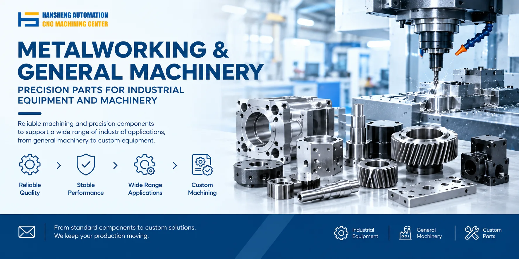
We can machine custom nozzles, fixtures, precision shaft parts, and other parts for laser cutting equipment from customer drawings, for single-piece or low-volume production.
Overall, laser wafer dicing is becoming a mainstream technology in advanced semiconductor manufacturing due to its non-contact nature, high accuracy, high efficiency, and strong material adaptability. Traditional mechanical cutting still has uses in simple scenarios, but it can no longer meet the needs of shrinking chip sizes and complex structure processing. As laser costs fall and processes mature, laser cutting market penetration will continue to rise.
Our custom precision component machining capability is not limited to wafer dicing equipment. Beyond nozzles, fixtures, and precision shaft parts for cutting equipment, we also machine medical device parts, food machinery parts, yacht precision components, RC car structural parts, and non-standard parts for filling machinery and printing machinery. Hansheng Automation works from customer drawings and production quantities to deliver single-piece or low-volume precision machining.