Wafer AOI is highly important for the following reasons:
Defect detection:
The purpose is to identify and locate defects on the wafer surface. During wafer manufacturing, various defects may appear, including scratches, particle contamination, and micro-cracks. If these defects are not detected and addressed in time, they can directly affect subsequent process steps, leading to lower yield and higher cost. AOI uses high-resolution optical imaging equipment and complex image processing algorithms to quickly and accurately detect tiny surface defects, helping ensure wafer quality.
Process control:
The purpose is to maintain process stability and consistency. Wafer manufacturing involves multiple steps such as lithography, etching, and deposition. Each step can introduce small variations that may accumulate and ultimately affect product performance. Through real-time monitoring and feedback, AOI systems help process engineers adjust manufacturing parameters in time and maintain high production standards.
Production efficiency improvement:
The purpose is to reduce human inspection errors and increase inspection speed and efficiency. Traditional manual inspection is slow and easily influenced by human factors, causing missed or false detection. AOI systems can operate continuously around the clock with high speed and precision, significantly improving production efficiency and inspection reliability while reducing manufacturing cost.
Data collection and analysis:
The purpose is to provide detailed inspection data to support production optimization and root cause analysis. Defect data and trend information from the production process are important for improving manufacturing processes and optimizing workflow. AOI systems can collect and store large volumes of inspection data, which can be used for statistical analysis to help process engineers identify potential problems and take corrective action.
Quality assurance:
The purpose is to ensure that final products meet customer requirements. Semiconductor products demand extremely high quality and reliability, and even a tiny defect can cause product failure. Through strict quality inspection, AOI helps ensure that every wafer meets quality standards before moving to the next process step, protecting final product performance and reliability.
In addition, wafer AOI equipment involves advanced technologies such as wafer surface defect visual inspection, autofocus, and 3D imaging. These technologies continue to develop and provide strong support for efficient and accurate wafer inspection.
Wafer surface defect visual inspection technology: Uses high-resolution optical microscopes and cameras to scan the wafer surface, then analyzes the captured images with advanced image processing algorithms to detect tiny surface defects.
Autofocus technology: Ensures image clarity through laser ranging, image contrast focusing, and multi-point focusing, achieving high-precision focus on the wafer surface.
3D imaging technology: Obtains three-dimensional structural information of the wafer surface, which is important for detecting and analyzing complex defects. Techniques such as structured light illumination, confocal microscopy, and interference microscopy can generate high-resolution 3D images for precise defect measurement and analysis.
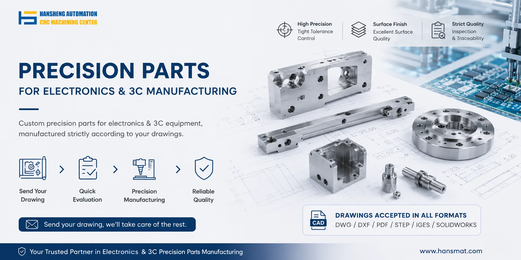
For non-standard mechanical components used in wafer AOI systems-such as precision motion stages, optical mounting brackets, or autofocus module supports-Hansheng Automation provides custom machining services based on customer drawings and required tolerances, helping maintain stable optical alignment and repeatable inspection performance in semiconductor manufacturing.